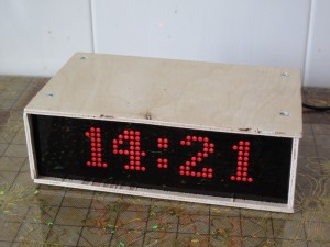
Fig 1. Finished Clock Prototype
I started playing with Arduino boards a while ago, and soon discovered an interesting IC, the Maxim DS3231. It is a chip that provides extremely accurate time, backed up with a small battery. Why is this important? Well, for quite a long time, consumer watches and clocks have been timed with a quartz crystal. This provides fairly good accuracy, but production processes have become very slack due to cost cutting, and very few of these will keep very accurate time. Sure, my cell phone has the time, but it’s usually laying around somewhere, or in my pocket. I like to just turn my head and check the time sometimes. So I like to keep a digital clock around, as well.
With an Arduino, I found that I could build a digital clock that is accurate to an amazing degree, only several seconds difference per month. As a bonus, I found that I could program it to handle time zones, and the dreaded change to and from Daylight Savings Time, automatically. So I began to build a long series of prototype clocks, based on many different kinds of displays. One of the most current versions used four 8×8 red LED matrix displays, and looked pretty cool. It became part of a system that also read and displayed weather information from Environment Canada’s data server.
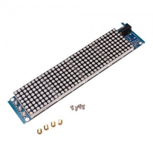
Fig. 2 – The JY-MCU PRO 3208 display module
Always scouring Ebay for new display ideas, I came across the JY-MCU PRO 3208 display, very new on the market. It has some advantages over the other matrix displays, including larger LEDs, an onboard AVR processor and provision for an RTC (not installed), and was better integrated as a display board, having proper mounting holes that the others lacked. So I ordered one up. When it arrived, I powered it up and it dutifully lit up with a digital clock face (provided by the internal firmware). But my goal was to customize it.
Expecting to find a plethora of software on the internet for it, I was horrified to discover that it was all supporting the previous version, the JY-MCU 3208 (no PRO). So after some aggressive back and forth with the Ebay seller, they finally provided me with a link to download the information package (all in Chinese!). Armed with a schematic and a library that they had copied from Sparkfun, I proceeded to fire it up. The first obstacle was that the processor is a tiny AVR, pin compatible with the well known 328p, but driven with a watch crystal instead of a resonator. This would make a direct upload from the Arduino IDE impossible without modifications.
However, it slowly dawned on me that the onboard processor and the HT1632 display driver IC both share the same programming port pins on the display. Furthermore, I could disable the processor with a single jumper wire. So it would be possible to attach the display to an Arduino and run much more interesting software on it. So off I went to the table saw in the basement, and cobbled up a box that would hold the display, and two Arduinos – a Mega 2560, and an Uno clone. The Mega was equipped with a protoboard piggybacked with a socket for a NEO-6M GPS receiver, and a JY-MCU DS3231 based RTC (real time clock) module. The reason for this giant overkill, was that I was heading for China, and would not have access to all my components and tools. So I provided everything with header pins, and took along a generous supply of DuPont female to female jumper wires. This way I could easily experiment and change things without much effort.

Fig. 3 – Inside the clock – top view
The box consists of four thin plywood sides, held together by two pine side supports. These supports also provide a backing to mount the display with four screws. A thin slot was cut with the table saw, just inside the front edge, to form an escutcheon to hold the display filters. I used high quality Lee photographic studio filters, both a gray and a red colour, to filter out internal reflections and increase contrast. I tested a lot of different filter combinations using the Lee filter sample book, to find the most effective combination. I have also added glass in some other prototypes, but didn’t want it breaking in my suitcase, so I just used the filter material, which is a little too floppy for such a big panel. I will fix that later. The display has more than ample brightness to overcome the light loss of the filter, and still appears “too bright” to my eyes at full brightness. It can be set to any of 15 brightness levels in software. I’m sure that running it at lower levels will also increase the LED life span.

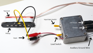
Fig. 4 – JY-MCU PRO 3208 External Control Connections
I’m going to tell you everything you need to know to build one of your own. The onboard AVR on the display is disabled by connecting a jumper from the pin on the display ICSP connector to an adjacent ground (on the display power connector), as mentioned above. This enables a connection to the HT1632 display driver on the same connector, which you can see in Figure 4, to the left. In this configuration, the module receives all its power and control signals from the Arduino. There are only 5 wires to connect, not including the jumper wire (blue in the diagram). There are more details about the hardware connections on the repository page that I link to further on. Before you get too excited about the GPS, we’re not using it for this project. I have developed software that can set the RTC automatically from it. Although it is currently running on the Mega, it will run perfectly well on the Uno. There is no good reason why it wouldn’t run on almost any flavour of Arduino. The circuit requires one DS3231 based RTC on the I2C lines, it doesn’t matter which brand.

Fig 5. Mounting and CPU connections
I had a real task cut out for me when I tried to write code for the board. The library that was linked to by the seller (by the way, I have no idea who wrote it or where it came from, but it appears to include the source code for the onboard clock, so I’m merely assuming that it is the manufacturer), displayed the characters in a cockeyed fashion, which I eventually determined is because the LED matrices are rotated clockwise. Thus rendered quite useless. So I inhaled deeply and began to modify the library. It turned into a four week task, working a few hours a day.
I began by writing set and clear pixel routines which are useful in their own right, and then created character and number display methods based on those. I discovered a good font for characters, the ANSI CP437 character set, which has its origin in the original IBM PC! For the clock, I improved the number 0-9 fonts and replaced some seldom used graphics characters with those. They look a lot more legible since they are taller and thicker. I only used them for the clock, if you print something with numbers they will match the letter set more.
Here is a link to my software repository, where you can download all the code – HT1632 Arduino Library for JY-MCU PRO 3208. The repository includes three application programs – A display test program, the clock program, and an implementation of James Conway’s incredible “Game of Life” which is a famous “cellular automaton” or mathematical creature simulator, if you like. There is also a small wiki documenting the class methods so you can use it to write your own programs.
Here, at the time of writing, is the link to the onboard firmware and schematic diagrams of the JY-MCU module – module documentation – click on “??(349KB)” (where the ?? are 2 chinese characters). To unpack the .rar file, you may have to install 7-zip.
The clock program is fairly sophisticated. It polls the RTC 10 times a second, hence can be accurate to 100 milliseconds when freshly set. It has a serial configuration program that allows the user to set the time and configure 12/24 hour time, time zone, a blink mode, and display some other internal registers that are sometimes of interest. The RTC must first be set to UTC or Greenwich time. Once set to a local time zone, the time rules for that zone are selected. This means that Daylight Savings Time is handled automatically and correctly. Basically, this clock is really a “set and forget” appliance, because, although specified to lose no more than about a minute a year, reports from the field indicate that it will usually outperform that, and deviate only by a few seconds. Compare that with most digital watches and clocks, which typically gain or lose many seconds a day.
I’ve been busy adding features. It now responds to button presses on an IR handheld remote. You can select different clock information, or the Game of Life. Another feature is auto brightness. It calculates the sun’s position in the sky and use that to set brightness according to the actual sunrise and sunset times at the clock’s location. There is an optical sensor in the back, as an alternative. The location is set from GPS inputs. That inspired me to also add lunar phases, which it keeps track of, but I’m not sure yet how to display. It also has a DHT22 temperature and humidity sensor, so that information can also be displayed.
I have working prototypes that automatically synchronize my clocks to GPS or atomic clocks on the internet. But those are in development and not yet ready for public release. Another working project I have, is a time server that broadcasts the time from a 433MHz low power transmitter, to all the clocks within a radius of approximately 100 meters that are equipped to receive it.
Another aspect of the overall effort is more artistic – to make clocks that are beautiful and distinctive. I have begun to experiment with finished wood enclosures and different colours and unusual display formats that look cool. The styling on this one came off too much like a shop sign, so I’m eyeing some smaller 8×8 LED modules in different colours like blue and white. They are not available in OEM units with integrated drivers, so I’ll have to build them almost from scratch.


